Views: 0 Author: Site Editor Publish Time: 2026-07-01 Origin: Site


Protective films can look almost identical on a production line, yet their performance around sensitive electronics may be very different. Standard film mainly guards against scratches, dust, fingerprints, and handling damage, while ESD protective film is designed to control electrostatic risk during application, movement, and removal. Low-charging, dissipative, and discharge-shielding properties are not interchangeable, so an anti-static protective film should never be selected by label alone. The sections ahead compare how each film behaves, where ESD protection film is genuinely needed, and which electrical and adhesive specifications should be checked before purchase.
Both film types can form a temporary barrier against abrasion, dust, fingerprints, and minor handling damage. Standard film is the correct choice when the risk is mainly cosmetic or mechanical. Its performance depends on stable coverage, suitable adhesion, and clean removal. Typical substrates include glass, painted metal, plastic panels, and appliance housings.
ESD protective film adds a second responsibility. Along with preserving appearance, it must reduce electrostatic risk around sensitive components, assemblies, or exposed circuitry. This damage may be immediate, but it can also remain latent and escape initial inspection before causing premature failure later. Electrostatic damage can occur during manufacturing, testing, shipping, handling, installation, and field service.
Standard protective film is therefore not an inferior version of an ESD product. It is a material designed around a different failure mechanism. A scratched panel, contaminated surface, or adhesive residue can normally be identified during inspection. Electrostatic damage may leave no visible mark, making electrical behavior part of the protection requirement whenever sensitive electronics are exposed.
Ordinary polymer films are often insulative, which allows charge to remain on a surface after contact and separation. An anti-static protective film is engineered to alter that behavior, but its exact capability depends on the material construction and test results. Low-charging performance reduces the amount of triboelectric charge produced. Dissipative or conductive performance provides a path for accumulated charge to move when the material is used within an appropriate grounding system.
Discharge shielding is a separate property that limits energy from an external electrostatic discharge reaching the protected item. It usually requires an engineered packaging structure, so an anti-static surface film should not be assumed to provide shielding. Low charging, resistance, and shielding are separate properties, and low-charging behavior cannot necessarily be predicted from resistance alone.
Terms on a datasheet should therefore be read precisely. “Anti-static” may refer only to reduced charge generation, while “dissipative” describes a resistance range that allows charge to move more gradually. “Conductive” describes still lower resistance, and “shielding” concerns protection from a discharge originating outside the package. One claim does not automatically establish the others.
Comparison point | Standard protective film | ESD protective film |
Primary purpose | Prevent physical and cosmetic damage | Combine surface protection with electrostatic control |
Charge generation | Usually not specified | Designed for lower charging behavior |
Charge movement | Normally remains insulative | May be dissipative or conductive |
Discharge shielding | Not provided | Only available in a structure designed and tested for shielding |
Typical applications | Glass, metal, plastic, painted panels, appliances | PCBs, displays, sensors, connectors, and electronic assemblies |
Main buying evidence | Adhesion, thickness, durability, clean removal | Electrical data plus adhesive and substrate compatibility |
The practical difference is not simply “static protection versus no protection.” Buyers must identify the required electrical behavior and verify that the film has been tested for it. Even an ESD protection film may be unsuitable if it offers low charging while the process also requires dissipation or shielding. Appearance, film color, and a general anti-static label cannot replace property-specific data from the supplier.
An ESD protective film should be evaluated when the protected surface is attached to or handled near an electrostatic-discharge-sensitive assembly. Examples include printed circuit boards, flexible circuits, semiconductors, sensors, connectors, display modules, touch panels, and electronic subassemblies. Risk is especially relevant when film is removed near exposed circuitry, because a layer that prevented scratches may still generate charge during separation.
Industry category alone is not enough to make the decision. A metal appliance panel may need only scratch protection even though the finished product contains electronics elsewhere. Conversely, a small decorative layer may require anti-static protective film if its application or removal occurs within the critical handling zone of a sensitive component. The deciding questions are how vulnerable the item is, how close the film comes to it, and whether the process generates or transfers charge.
The existing ESD-control plan should also shape the specification. Where grounded operators, dissipative work surfaces, ionization, and controlled handling are already in place, the film must integrate with those measures rather than undermine them. A highly charging film can remain a concern even when other parts of the workstation are properly controlled.
Standard film remains the practical option when electrostatic exposure is not meaningful and the main concerns are scratches, abrasion, dust, fingerprints, paint overspray, oil, or transportation marks. A versatile PE or PET surface protective film is commonly suitable for glass panels, metal sheets, plastic housings, household-appliance surfaces, automotive trim, fabricated parts, and construction materials. In these cases, adhesion stability, conformability, weather exposure, film thickness, and clean removal usually matter more than electrical resistance.
Specifying ESD protection film without a defined electrostatic risk can add cost and process controls without improving the product. Establish the failure mechanism first: standard film suits visible mechanical risks, while charge generation, electrostatic fields, or direct discharge require electrical performance in the specification.
A mixed product may require both approaches. Exterior panels can use standard protective film while sensitive internal modules receive ESD-controlled materials and packaging. Separating the requirements by component prevents unnecessary specification complexity without leaving vulnerable parts unprotected.
Location within the handling process changes the required protection. Inside an Electrostatic Protected Area, packaging and handling materials used with sensitive devices generally need to be low charging and dissipative or conductive. Outside that controlled area, the packaging structure may also need electrostatic-discharge shielding.
This prevents a frequent purchasing error. An adhesive anti-static protective film may reduce charge generation at the surface, but it is not automatically complete transport packaging. Sensitive goods leaving the controlled environment may need a separate qualified shielding system.
IEC 61340-5-3:2022 covers protective packaging properties for ESD-sensitive devices across production, rework, maintenance, transport, and storage. Its scope supports a system-level decision rather than reliance on a broad “ESD-safe” claim.
The surface film and outer package should therefore be specified separately. One controls what happens at the protected surface during processing or removal; the other may need to protect the complete product from external discharge during uncontrolled transport and storage.
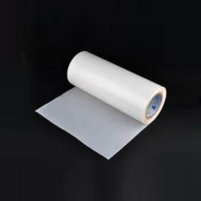
Product names are not proof of performance. Ask the supplier to identify the measured property, test method, conditions, and treated side or layer. Relevant documentation may include surface or volume resistance, triboelectric charging, charge decay, and shielding data when shielding is claimed.
Each measurement answers a different question. Resistance describes charge movement, low-charging tests examine charge generation, and charge decay measures how quickly charge falls under defined conditions. Shielding tests evaluate energy transferred into a package, so resistance alone cannot prove shielding.
Buyers should also confirm where the treatment is located. The exposed film surface can affect charging during unwinding and handling, while the adhesive-facing surface influences contact with the protected part. A product treated on only one side may behave differently when orientation changes. Double-sided control should be verified rather than inferred from a general ESD protective film description.
Also review humidity, aging, abrasion, cleaning, and storage conditions. Some treatments are more sensitive to moisture or surface wear, so a favorable result on a new sample may not represent performance after storage and handling. Request data that reflects the production environment.
Review electrical data together with the physical application. Define the substrate, coating, surface texture, cleanliness, protection period, temperature, humidity, chemical or UV exposure, line speed, peel rate, and acceptable removal force. A film suited to polished glass may lift from textured plastic or bond too aggressively to a delicate coating.
The selected ESD protective film must also fit the control system. A dissipative material needs a valid path to ground, while an insulative surface near a sensitive device may require ionization. A complete ESD-control program should cover manufacturing, assembly, packaging, inspection, handling, and transport rather than treating the film as an isolated solution.
A concise supplier checklist should cover:
● Electrical property, classification, and test method
● Test humidity, temperature, aging condition, and sample orientation
● Treated surface or adhesive layer
● Substrate compatibility and recommended tack
● Peel adhesion before and after aging
● Residue, staining, and coating-lift results
● Intended use inside an EPA, outside an EPA, or within transport packaging
These questions should be answered for the exact film construction being purchased. Results from another thickness, adhesive formulation, treatment level, or base polymer may not represent the supplied product. When a film is customized, qualification data should match the finished specification rather than a generic product family.
Final approval should come from a trial using the real substrate and production method. Apply the film after normal cleaning, run it through the intended equipment, age it for the expected period, and reproduce handling or transportation. Include the lowest realistic humidity and remove the film at the intended angle and speed.
Observe bubbles, wrinkles, edge lifting, residue, staining, and finish changes. Electrostatic measurements should cover unwinding, lamination, movement, and removal near the sensitive item. When the film is part of a larger package, test the complete system under the conditions expected across the handling lifecycle.
A trial should use the same roll width, film tension, application pressure, line speed, and removal procedure planned for production. Small hand-applied samples may be useful for initial screening, but they cannot reproduce every source of charging or mechanical stress on an automated line. Multiple samples should be tested after realistic aging to identify inconsistent adhesion or electrical performance.
Set acceptance criteria before the trial: maximum peel force, allowable defects, electrical classification, charging behavior, and any shielding requirement. Record the test instrument, probe arrangement, environmental conditions, sample conditioning, and measurement timing so later batches can be checked against the same method rather than compared through visual inspection alone. A successful sample must meet both physical and electrical criteria after realistic aging. That turns “anti-static” from a label into a verifiable production requirement.
Production approval should also define how continuing performance will be monitored. Supplier certificates, incoming inspection, periodic resistance measurements, and peel testing can help identify changes between batches. The level of verification should reflect the sensitivity of the protected device and the consequences of a failure.
The right film depends on the risk you need to control. Standard protective film is usually sufficient for scratches, dust, and handling damage, while ESD protective film is necessary when application, movement, or removal could expose sensitive electronics to electrostatic charge. Labels such as anti-static protective film should still be checked against electrical data, adhesive performance, and real production conditions. CHUZHOU TAILAI IMPORT&EXPORT TRADING CO.,LTD. supplies surface protective film materials and application-focused support, helping manufacturers match adhesion, removability, and substrate compatibility to practical requirements while keeping protection processes efficient and reliable.
A: Standard film primarily prevents scratches, dust, and handling damage. ESD protective film adds controlled electrical properties that reduce charge generation or help dissipate static near sensitive components.
A: No. Anti-static properties usually reduce charge buildup, while discharge shielding requires a specially engineered structure. Buyers should verify low-charging, dissipative, conductive, and shielding claims separately.
A: It is commonly needed when films are applied, moved, or removed near circuit boards, semiconductors, sensors, displays, connectors, or other components vulnerable to electrostatic discharge.
A: Yes. Ordinary polymer films can accumulate charge through contact, friction, and separation, particularly during unwinding or peeling. This does not make them unsuitable for non-ESD-sensitive applications.
A: Review documented surface or volume resistance, triboelectric charging, charge-decay results, treated-side information, and test conditions. Final approval should include trials on the actual substrate and production process.


